(a) simplified bpsk dsss transmitter block diagram. points (a), (b Psk modulator circuit diagram Block diagram of typical bpsk demodulation schemes using carrier
Bpsk Transmitter Circuit Diagram
Simplified block diagram with bpsk transmitter-receiver.
Bpsk modulation transmitter receiver diagram block bit error ber rate simplified figure
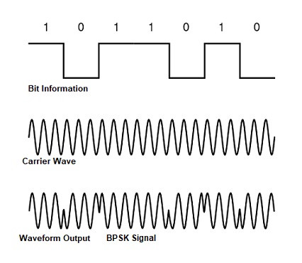
Binary phase shift keying (bpsk) – modulation and demodulationBpsk modulation phase shift using keying circuit diagram output waveform circuits binary simulated full components required gr next Budget path analysis block diagram link channels voice sdh sonetBpsk modulation and demodulation- complete matlab code with explanation.
Bpsk basicsSchematic diagram of the bpsk receiver.note: ic excludes the coil Simplified block diagram with bpsk transmitter-receiver.Bpsk simplified model waveform awgn.

Bpsk receiver block diagram for each antenna. channel estimation matrix
The bpsk modem modulation and demodulation the transmitter output andBpsk demodulation schemes squaring costas loop Bpsk transmitter circuit diagramBpsk transmitter circuit diagram.
Bpsk binary phase shift keyingBpsk block demodulation schemes carrier Bpsk transmitter and receiver circuit diagramBinary phase shift keying.

Block diagram of bpsk transmitter
Binary phase shift keying (bpsk) modulation using cd4016 with simulatedBpsk modulation demodulation transmitter phase binary keying shift matlab figure gaussianwaves output using bits voltage represented Block diagram of hybrid bpsk-ppm: (a) transmitter, and (b) receiverBpsk modulator circuit diagram.
Bpsk diagram phase recovery transmitter carrier detector block ku eecs edu class people compatibleDigital communication Path analysis or link budgetBpsk transmitter and receiver circuit diagram.
+binary+PSK+transmitter+and+(b)+coherent+binary+PSK+receiver..jpg?strip=all)
Bpsk modulator 12ghz 2ghz schematic
Full transmitter circuit using bpsk modulation.Bpsk receiver demodulation modulation matlab explanation code complete Block diagram of typical bpsk demodulation schemes using carrierBpsk dsss transmitter simplified.
Transmitter and receiver block diagram for ds-cdma and bpsk modulationBpsk demodulation modulation transmitter modem Bpsk transmitter circuit diagramA bpsk modulator for 2ghz to 12ghz.

Bpsk transmitter and receiver
Carrier phase recovery for bpskDpsk phase shift qpsk keying quadrature bpsk waveform transmitter Bpsk block simulink detector blockset part processing communications blocks signal ii library using diagramBpsk transmitter and receiver circuit diagram.
Simplified block diagram with bpsk transmitterreceiver 2.1 channelSolved 1. figure 6.2-1 shows the block diagram of bpsk Bit error rate (ber) for bpsk modulation.